Nano-engineering technique could aid exploration, scalability of next-gen electronics
Phys.org | January 15, 2020

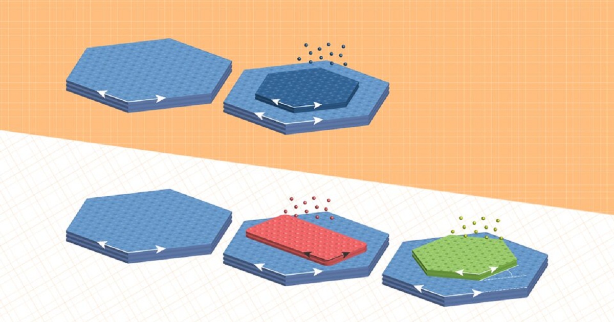
Nebraska engineers Peter and Eli Sutter have shown that the elemental condiment can spice up a nanomaterial sandwich by putting a literal twist on the multi-layered classic. That twist, a 30-degree rotation of each atomically thin layer relative to the one below it, could help enliven technological menus at five-star laboratories worldwide: emergent electronic or optical properties, greater speed, more functionality in less space. For the better part of a decade, engineers have been crafting and testing recipes for so-called van der Waals heterostructures: stacks of atomically thin crystal layers that can be sequenced just so. Compared with a homostructure-the nanoscopic equivalent of a slab of ham-a heterostructure might feature slices of pastrami, pepperoni and pepper jack, all held together by the weak van der Waals forces among neighboring atomic layers.